
Overview
I'm writing this document in the hopes that it will help those who are struggling to sift through the gigantic 1270 page manual for the PXA270 microprocessor. While initially configuring mine, I spent a good deal of time figuring out why software and hardware interrupts were behaving strangely or not working at all, where the interrupt vectors lived at, and how I could get the Micrium OS-II operating system to work with this thing.
As a little bit of background, I am running the Intel XScale PXA270-10-520 processor with a Starter Development Kit (SDK) board from Zoom Logic. I am compiling my instructions with the IAR ARM compiler running on an old Dell laptop, and they're written partly in C and partly in assembly. The reason for the latter is that the Micrium OS-II requires you to write your own functions for placing the processor registers on the stack and taking them off again in case the OS needs to switch tasks (multi-thread) or gets interrupted by software or hardware. Later on I'll talk more about this and provide port files that should work if you're using the same architecture.
For a mapping of the register names to hexidecimal values, see the file bsp.h linked below.
Serial Port (FFUART)
- Getting interrupts to work with the FFUART serial port on the chip was a real headache.
In addition to making sure that the FFUART is not masked in the interrupt IRQ controller
REG32[0x40D0_0004] |= BIT22
you must also enable the 64 character FIFO mode for the Receive Buffer Register (RBR) and set the proper interrupt bits in the FFUART Interrupt Enable Register (IER). In my case, I wanted an interrupt to occur whenever receiver data was available (trigger threshold reached), so I setREG32[0x4010_0004] |= BIT0
And finally, the really tricky--you gotta read the fine print and pay attention to every single detail one--was that you have to set the interrupt enable bit in the Modem Control Register.REG32[0x4010_0010] |= BIT3
- Enabling Flow control with CTS and RTS also proved to be more difficult then it should have
been. The reason? I wasn't smart enough to realize that the LOLO bootloader program was not
enabling the GPIO pins for the CTS and RTS signals.
The schematic for the PXA270 SDK shows the TX, RX, CTS, and RTS lines for
uP_FFUARTA all hooked up to the DB9 connector on the SDK board, so I just assumed that the CTS and
RTS lines would be enabled by default. When I printed out the values of the GPIO Alternate Function
registers, though, I found that they weren't configured to route CTS and RTS to the pins on the
DB9 connector.
To enable the FFUARTA pins to do handshaking properly with the configuration on the SDK, you need to do the following:GPIO_ALT_DEF_32_47_REG_ADDR = 0x00088058; /* Set GPIO 34,35,39,41 alt. functions for RX, CTS, TX, RTS, resp. */
GPIO_PIN_DIRECTION1_REG_ADDR = 0x000202C2; /* Set GPIO 32,38,39,41 and others as output pins (RTS) */
Of course, you may want to enable additional GPIO pins, in which case your settings would be different.
- Losing Bytes over FFUARTA TX to Windows PC RX was a major problem that I was encountering way too
often when I would try to transmit large amounts of data and log it to a file on my PC. At first I thought
that the Tera Term program that Logic recommends using for serial port communications was the culprit since
RealTerm could send the data without losing bytes. When using Tera Term, for 2 MB of data sent,
I'd typically lose 1-10 bytes.
However, after switching PCs, I fond that both Tera Term and Real Term work just fine. It turns out that the ancient 2003 Dell Latitude laptop I was using was the real culprit. My recommendation: Don't use an old, slow laptop!!. I'm not sure if it was the drivers for the serial port or the actual hardware and handling of the buffer, but it was a definite problem.
OS Timers
It doesn't seem to be listed anywhere in the manual, and it's most likely a result of the firmware initally loaded by the Zoom development kit, but OS Timer 4 is initially enabled as a source of interrupts to the processor. This took me some time to figure out, and it took me even more time to figure out how to service the interrupt.
The second task that was somewhat confusing was getting the 1 ms and 1 s clock ticks working. It turns out that you have to enable the 32.768 kHz clock manually by setting OSCC[OON] and then waiting until OSCC[OOK] is set high. The exact steps are well described on p. 108 of the PXA270 Developers Manual, but it took me a while to find this exact section.
Port Files for MICRIUM OS-II on the PXA 270
While the Micrium site does offer some useful application notes (AN-1011 and AN-1018 are probably the most helpful) to help one in getting started with a port, it does not provide a full port for the PXA 270 processor. Furthermore, the application notes do not provide a complete prescription of how to produce a port for the PXA 270, and they disagree in some areas. For instance, one note tells you to push both CPSR and SPSR onto the stack during a context switch while the other tells you to only do so for CPSR. The textbook "MicroC/OS-II: The Real Time Kernel, Second Edition" by Jean J. Labrosse helps to make up for areas where these notes fall short. But it adds a touch of its own complication by using different file and function names than those used in the application notes.
Reading through all this material helped my understanding of what is going on inside the processor and OS quite a bit. However, I would have gladly taken a full port if someone had offered it to me. Here are the C and assembly files one needs to successfully port Micrium to the PXA 270. Note that while the files contain all the necessary instructions and registers to get you going, you will definitely have to tailor them to your application. Also, I've included the files as they were while I was debugging things, so there are a lot of unecessary print statements and LED flashing and whatnot.
- bsp.c : This file contains a function called BSP_InitIntCtrl that should be called at the beginning of your application to set interrupt vectors, enable timers and serial ports, etc. It also has the C code that handles interrupts from the peripherals (Note the text refers to the OSTickISR function referred to in the text is covered by OS_CPU_IRQ_ISR_Handler).
- bsp.h : In this file are the register addresses used throughout the code I provide.
- os_cpu_a.s : This is the file that has all of the ARM assembly code necessary to handle context switches.
- os_cpu_c.c : In this file you'll find the initialization of the stack from the function OSTaskStkInit and the optional hook functions for MICRIUM.
- os_cpu.h : The typedefs for the ARM architecture and the interrupt disabling and enabling macros are defined in this file.
Port Files for MICRIUM FileSystem Module and Compact Flash on the PXA 270
In my application, I'm using the Micrium Filesystem (FS) module to read and write files on a compact flash (CF) card. The Logic SDK kit contains an onboard compact flash drive and a specialized IO controller chip that handles most of the signals that are necessary to drive the controller on the card. So there's no need to break out the soldering iron or play with jumpers to get the thing working; only writing some software.
Now, if one has experience with memory mapped peripherals and IDE controllers and writing device drivers, reading and writing a file on the CF card might not be that challenging. But if that's not the case, this can be a difficult task. Part of the challenge is knowing where to look to get the information you want. The PXA 270 manual has a long, well written section about the CF interface, but unfortunately, most of it is useless if you're trying to get the drive on the SDK board working. That's because the IO controller does most of the work for you. And also, it doesn't provide any sort of description of what "Attribute Memory Space" or "Common Memory Space" actually is.
Instead of trying to explain these things myself and potentially doing a lousy job, I'll point out the references I found useful. This Circuit Cellar Article on Compact Flash cards is an excellent, concise start to Compact Flash. The CompactFlash Specification Manual will give you the finer details of how to write the configuration registers and interpret the Card Information Structure (CIS), which lies in Attribute Memory Space. And this XiLinx Application Note provides an excellent guide to the Attribute Memory, Common Memory, and I/O space.
For the case of the Logic SDK Kit, the address range 0x14000000-0x14FFFFFF has been mapped to the off-board CompactFlash Type 1 Memory Only
Slot. The uP_MA[12] line is actually connected to the REG line on the controller, which means that when an address starts with
0x14000___, we are accessing configuration registers and the CIS, and when the address starts with 0x14001___, we are accessing
common memory space. The latter is the space we want to write/read to get the data off the Compact Flash card. The former will
tell us about the card itself (how big the sectors are, how many there are, etc.). It's a pretty informative exercise just to
read all the values in the 0x14000___ to 0x14001___ range to see how this all works.
The process of actually reading and writing data from/to the card is a little tricky. And rather than try to explain where to wait
for status bits to flip or how to write the ATA registers to set up a read/write, I'll just provide a Compact Flash driver I wrote
for the Micrium FileSystem module. You'll need the registers defined in bsp.h. The files
fs_dev_cf_card.c and fs_dev_cf_card.h
show how to manipulate the Compact Flash card.
SD Card Interface in SPI Mode
Programming the SD Card controller to operate in SPI mode is a little bit of a challenge, mostly because the documentation in the PXA270 manual is very poorly organized (in my opinion, at least). I will try to sum up the most important things that I learned and correct the documentation where necessary.
1) For starters, the PXA manual says conflicting things about what software (i.e. you) have to do with the Chip Select (CS) signal. It implies that you have to manually turn the signal off in between commands. If you try this, you won't have success. It turns out that you needn't do anything with the CS signal once you've activated it in the MMC_SPI register. The controller will assert the signal as necessary when it issues a command.
Quick Capture Interface and DMA
There are several very tricky issues one must consider when trying to get the Quick Capture Interface (QCI) to write buffers using DMA. The biggest speedbumps I encountered were 1) configuring the DMA descriptors for the QCI properly, 2) writing the DMA registers in the proper order, and 3) getting the DMA to work consistently on a buffer in memory. The secret to the last one was something I probably wouldn't have figured out for weeks if a friend hadn't diagnosed it as a cache-related problem. As I now know, DMA and cache are always going to be problematic on your standard microprocessor because the CPU doesn't know that the values in physical memory have changed when DMA writes them.
-
1) DMA Descriptors : On page 1182 in section 26 of the PXA Developer's Manual, they lay out a five step process to
get the QCI working with DMA requests. There are several useful instructions here. However, they write steps 1 and 2 as if you
would be programming DMA with non-descriptor fetches, stating that you only have to program DTADR, DSADR, and DCMD to get
the transfer set-up. Non-descriptor fetches can transfer a maximum of 8K, though, so that would have to
be a pretty damned small camera to get an image out. If you want to set things up for a realistic camera-say 4 megapixels-you
have to use descriptor based fetches.
For those of you who are unfamiliar with DMA descriptors, think of them as a big chain of target addresses (DTADRs), source addresses (DSADRs), and command addresses (DCMDs). Say we're using channel 0. For that channel, we have to make the DDADR register at 0x40000200 point to the first link in the chain, like in the figure below, which is 32 bit memory address that contains a value that will loaded into DDADR after the first DMA fetch takes place. The three 32 bit memory addresses following contain the values that will be loaded into DTADR, DSADR, and DCMD for that fetch. After this first fetch takes place the DMA channel jumps to the next DDADR and loads the next DTADR, DSADR, and DCMD for the next fetch. And so on, and so on.
I only show the addresses of the descriptors below. For an example of the values one would write to these memory cells, see bsp.c.
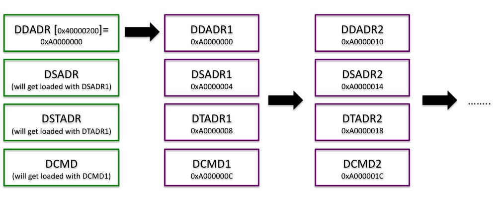
Each of the DCMDs in the chain should transfer LEN bytes, and once this amount has been transferred, the LEN bits will be decremented to zero. The last DDADR in the chain should be 0x00000001 to signal that the transfer is done.
- 2) Order for Writing DMA Registers : This was partly my fault for not reading instructions carefully enough and partially the fault
of Marvell for not spelling things out clearly enough. Now, this has to do mostly with non-descriptor transactions, so it's not necessarily
the most useful for getting a full image captured. But for debugging purposes, I wanted to start out with transferring just 1K of data from
the QCI to a buffer, so I chose to start with a non-descriptor fetch transfer.
On page 209 of the manual in section 5, it states that the first thing that should be done with configuring a channel is to clear DSCRx[RUN] and then write DCSRx[NODESCFETCH]. If you program DTADR, DSADR, or DCMD before doing so, the values you wrote will not stick after the write takes place. This makes sense since these three registers are reserved when DSCR[NODESCFETCH]=0, but that's in hindsight. At the time it wasn't clear to me that this should happen.
- 3) Disabling Cache for 1MB Sections on an ARM Processor : Like I said, I probably wouldn't have figured this one out for a long time
if a friend hadn't helped me out. I was pretty certain that I had all of the DMA and QCI settings configured properly, and I wasn't getting
any errors in the status registers when I would do an image capture. I didn't have an actual camera to work with at the time, so the best
I could do was use the QCI to fill a buffer with 0's. The buffer was just an array I declared in an include file, and it's the address
of this array that I fed to the DMA descriptor chain.
I'm going to describe the symptoms I saw in the next paragraph just in case someone reading this happens to have the same problem. If you already know you have a DMA-cache issue and you want to solve it, then skip it.
To test this out I used a simple dummy program where I could press "a" on the keyboard to fill the buffer with 1,2,3,4..., "b" to run the quick capture (which would fill the buffer with 0's), and "c" to print out the buffer. At first I thought it was working because I could press "a" then "b" then "c" and I would see all zeros, which meant that the 1,2,3,4 sequence had been overwritten. But if I tried it again I was stuck with 1,2,3,4... and couldn't get the QCI to overwrite the buffer anymore. What was happening is that the CPU was taking the values for the print from cache instead of reading them from memory, so that no matter what the real buffer value was, I only saw 1,2,3,4, etc. Thus began my adventure into disabling cache in regions of memory.
Disabling cache for the DMA buffer might have been one of the most difficult things I've done on a microprocessor or microcontroller. I couldn't find any examples that came with an explanation of how things worked. So hopefully I can provide you with one and save you the trouble of thinking too hard.
First off, I should say that now that I understand how things work, the Intel XScale® Core Developer's Manual and ARM Architecture Reference Manual actually do a pretty good job of explaining how the Memory Management Unit (MMU) works and how you can taylor it to disable cache or lock the Translation Lookaside Buffer(TLB). But at the time my response to reading these documents was "huh?" I'm not going to try to rewrite or paraphrase either of these two documents. What I will do is tell you how to disable cache and buffering for certain 1MB regions of memory.
Why 1 MB? Because that's the largest region, labeled a section, you have individual control over in the MMU Section Tables. There are smaller denominations called pages that allow fine control down to 1kB (tiny pages), but in the PXA270 there is enough memory to block off a big chunk of 64 MBs as uncached so that that kind of control isn't necessary. The section table, or Translation Table, is located at the physical address stored in the Translation Table Base Register (CP15, register 2). Since each 32-bit entry in the table corresponds to 1 MB, we need 4096 entries to span the entire 32-bit address space of the PXA270. So if I obtain the physical base address for the Translation Table in assembly like so,
PUBLIC Return_MMU_Table_ADDRand then call this function from C,
SECTION `.text`:CODE:NOROOT(2)
CODE32
Return_MMU_Table_ADDR:
MRC P15, 0, R0, C2, C0, 0 ;Get the value of the Translation Table Address
BX LRINT32U MMU_SectionTableAddr;I can print out all 4096 elements from address MMU_SectionTableAddr to address MMU_SectionTableAddr+4*4096 and see how the memory is being mapped, what areas are cacheable and bufferable, etc. So, for instance, if my table is located at 0xA0048000, I might see something like the following:
MMU_SectionTableAddr = Return_MMU_Table_ADDR();
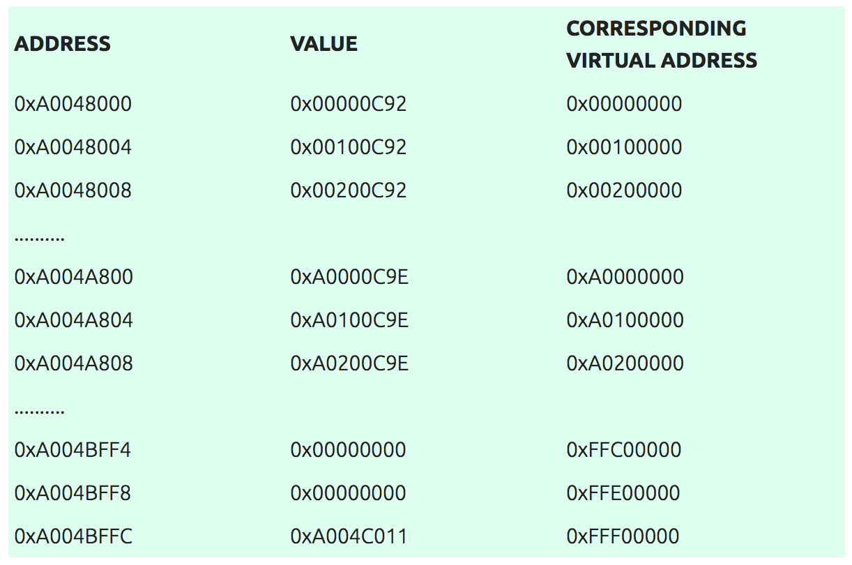
This shows that the beginning of memory is uncached and unbuffered and arranged with first-level table descriptors. Later on, in the section I'm using as RAM, I see that bits [3:2] are set, indicating that it is cached and buffered. And near the end there are empty sections that are mapped as invalid, followed by a coarse level descriptor at the final entry in the table (this re-maps the exception vector table: see the next section).
Now, I tried to simply modify this table in place and then invalidate the I and B bits in the TLBs, but this didn't work. Rather than beat my head against the wall trying to figure out why, I decided I'd try something simpler. So what I ended up doing was copying the table to a new section of RAM, making the modifications to the C and B bits in the address range 0xA3000000-0xA4000000 and then invalidating the bits and writing the new Translation Table Base Address to CP15. And sure enough, the cache is disabled for the arrays I want! To see how I did this, you can look at the function Update_MMU_Table in os_cpu_a.s.
The Exception Vector Table
The exception vector table is a set of 7 registers that determine how to handle things like interrupts and undefined instructions that may arise while the processor is running. It normally lives at 0x0000_0000. But in the ARM architecture, there is a bit in the C1 Control Register that can be used to move the table to 0xFFFF_0000. And if it's moved there, it can be re-mapped through the MMU to any address in RAM that you see fit.
So first off, here's what the exception vector table looks like:
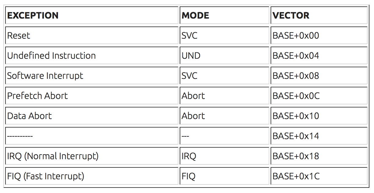
A more detailed table can be found at this ARM Exception Website. For our purposes it will suffice to say that at each one of these memory addresses there should be an appropriate instruction to handle its exception. For instance, in the bsp.c file above, you'll see that the instruction is to jump by 0x18 memory addresses to the memory cell that contains the address for the software interrupt handler. So whenever there is an interrupt from the serial port or QCI or whatever else, the software interrupt handler will be called.
You'll see many references that simply neglect to list the BASE address in the above table, leading you to believe that the vectors live at 0x0000_0000-0x0000_0020. But as mentioned above, they can be relocated to 0xFFFF_0000 by changing bit [13] of the C1 control register. To get this register, you'd execute the assembly instructions
                    MRC    P15, 0, R0, C1, C0, 0


                    ORRS   R0, R0, #0x00002000


                    MCR    P15, 0, R0, C1, C0, 0
I did not realize that my exception vector table had already been relocated to 0xFFFF_0000 for quite some time. It turns out that the Logic Loader program that runs on the Logic SDK system I have does this at startup.
When I was first getting my code up and running, before I had realized any of this, I had read somewhere that the exception vector table might live at the start of RAM (0xA000_0000). So I took a shot at writing the code for the exception vectors at 0xA000_0000-0xA000_0020, and sure enough, things worked as expected. And all the while, I was unaware that the address space 0xA000_0000-0xA000_1000 is actually mapped to 0xFFFF_0000-0xFFFF_FFFF.
The key to understanding this is to look at the last address in the MMU Table from the previous section. That is, at the virtual address of 0xFFF0_0000, we see the value 0xA004C011. Since bits[1:0]=1, this tells us it is a coarse page table base address and the coarse table lives at 0xA004_C000 (it must start on a 1kB boundary, i.e 0x000, 0x400, 0x800, or 0xC00). If we look at the memory from 0xA004_C000-0xA004_C3FF, we can see all the entries in this coarse table and how the re-mapping takes place.
All the address in the table are 0's except for one at 0xA004_C3C0:
[0xA004_C3C0] = 0xA000_0002
Since each entry in the coarse table is 4 kB, it takes an entire 256 entries to cover the whole table (note that this is a 1k virtual address range, with each entry separated by 4 bytes, so each entry maps to the one before+0x4000). And the table entry at 0xA004_C3C0 lines up with 0xFFFF_0000. Thus,
writing [0xA000_0000] = writing [0xFFFF_0000]
and this is why the exception vector table appears to live at 0xA000_0000 for the Logic Loader (LOLO) system. Moving it simply requires updating the final entry in the MMU Section Table with a coarse table address of your own. You'd want to use a 1kB coarse table entry, otherwise you'd be wasting a full 1MB of RAM.
JTAG Programming
The JTAG interface on the PXA270 consists of essentially 5 pins: TDI, TDO, TMS, TCLK, and NTRST. Here is a brief description of each pin.
- TCLK : Test Clock - a clock input for the Test Access Port controller and instruction and data registers
- TMS : Test Mode Select - controls operation of the test logic by receiving incoming data
- TDI : Test Data In - serial data input to the instruction and test data registers.
- TDO : Test Data Output - serial data output from either the test data registers or instruction register.
- nTRST : Test Reset - provides asyncrhonous initialization of the JTAG test logic.
There are many better and more in-depth explanations of these signals out there on the internet. However, each source seems to have its own advice about what pull-up resistors to use for each of these pins, especially for the nTRST pin. And this can cause a good deal of headache.
The PXA 27x Design Guide states that the for the nTRST pin, "an external source must drive nTRST before or at the same time as the hardware nRESET pin for correct TAP controller and device operation (pg 217)." In most cases, you will see people recommend using a 10 kOhm or 100 kOhm resistor to pull nTRST up. The problem is that if nRESET is also being pulled up by the same value, then there is no gaurantee that nTRST will be driven high before nRESET.
To get around this problem, I recommend using a lower resistance value for nTRST. While the exact values will depend on what sort of capacitance each pin is seeing, for the case of the Triton PXA270 daughter board, appropriate values are 100 kOhm for nRESET and 10 Ohm for nTRST.