Table of Contents
1.4: Synthesizing the Design in HLS and Exporting It
Now we get to the part where we start converting our algorithm into HDL and a hardware abstraction. HLS gives us the ability to synthesize our algorithm and build it from FPGA components like DSPs, LUTs, etc. without writing a single line of Verilog or VHDL!
1.4.1: Synthesizing GetCentroid
If everything from the previous section worked, you should be able to press the C Synthesis button (the little green arrow in the top toolbar) and begin synthesis. In a fairly short time (this is a very simple algorithm), you should see the following report:
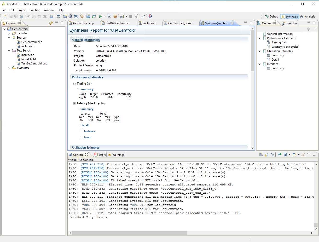
The first important thing to notice in this report is that it worked. No red text means we done did good :) If you see red text in the timing summary while you are working on a design, it means you are going to have to change your design to meet the timing requirements.
Here are some important things to note:
Timing: The timing closed with with the target clock of 10 ns, but it estimates that the actual clock period will be 8.47 microseconds. This means that we may be able to get away with running the algorithm more quickly!
It might not be obvious to folks that are unfamiliar with how this all works, but the Phase-Locked Loop (PLL) on the Zynq 7010 is capable of generating a range of primary clock frequencies. So you can do some iteration at this point and see how fast you can get things to go! To see if we can use a faster clock period, go to Solution -> Solution Settings, select Synthesis, and then change the Clock Period to 9 ns instead of 10 ns. Run the synthesis again, and you should see the following:
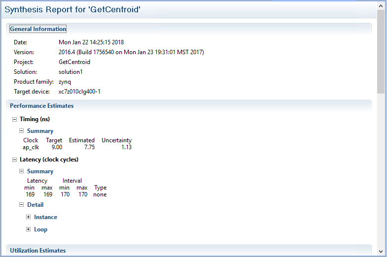
Notice that the Initiation Interval and Latency (more on this below) have the same number of clock cycles, but instead of a 10 ns clock period, we are running at a 9 ns clock period. We've increased our execution time by 10%! You can experiment with lowering the clock period more and seeing how fast you can get our centroiding algorithm to run.
Latency: the Latency is defined in UG-902 as the "Number of clock cycles required for the function to compute all output values." We can think of this as the execution time of our algorithm.
Initiation Interval (II): the Initation Interval is defined as the "Number of clock cycles before the function can accept new input data." This concept touches on one of the clear advantages of an FPGA design. The pipelined nature of the FPGA allows us to start operating on new data before the old data has been completely churned out.
The Latency and II for this design are both about 170 clock cycles. At 9ns, that means GetCentroid will take 1.53 microseconds between receiving its first waveform value and having a valid centroid for us to read in an output register.
1.4.2: Exporting GetCentroid
The final step we need to do in HLS is to export our design. When we do this, we'll turn our nice, compact C++ code into a much less compact collection of Verilog files (by default, HLS will also produce VHDL code). Before we move on, turn the clock period back to 10 ns since that's the clock period I'm going to stick with throughout the tutorial. After you've set the clock period to 10ns, click on Export RTL, the funky little orange box with the crosshairs on the top toolbar. This will bring up a window with options. We can use these options to change the RTL from Verilog to VHDL, place and route the design, etc. We'll stick with the default settings for now.
After clicking OK, assuming everything goes to plan, you should get a message in the bottom window of the console telling you that the RTL export has finished. If you didn't alter the solution name and you stuck with Verilog, you can find the four output Verilog files in C:\VivadoExamples\GetCentroid\solution1\syn\verilog. I think it is pretty darned instructive to take a look at these four files and see how the design looks in RTL. I guess it depends on how much patience you have (and whether your boss/teacher is waiting for you to turn something in).
Looking at these files will probably also make you want to personally thank the folks at Xilinx that made it possible to create a complex design with just a few dozen lines of C++. I know I do! It's really pretty incredible stuff if you have a think about it, as my colleagues in the UK say.
1.4.3: Using Our IP
You may be pleased to know that in the last step, we actually created our own Xilinx IP! We'll be able to make use of it when we build our full design in Vivado Design Suite. That's the subject of the the next chapter.
← Previous ... Next →