3.0 Adding the Memory Interface
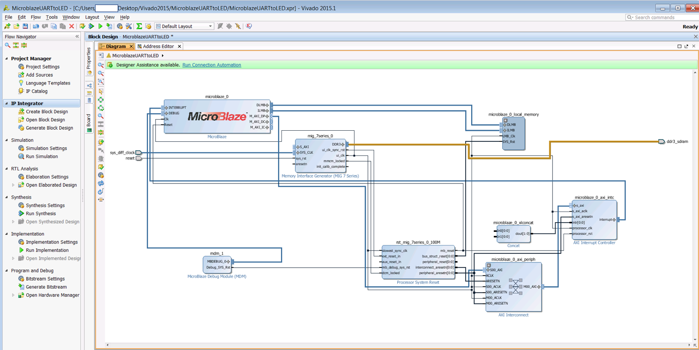
The first thing we need to do is add some RAM to our processor so we can actually do something with it. To do this, click on the Board tab in the Board Window and select the DDR3 SDRAM IP. Drag this onto the block design and you should see the following:
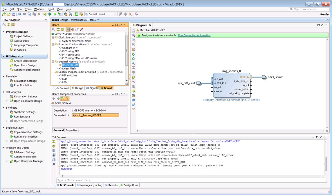
Notice that the SDRAM is called the Memory Interface Generator (MIG). This makes sense since we are literally generating memory with the internal logic of the FGPA. The next step is to click on the Run Connection Automation link that pops up at the top of the Block Design. This will be the general trend after we add a new component. Just be very thankful that Vivado is smart enough to know how to connect things so we don't have more places where we can mess up! Having said that, you still have to be careful that it does what you want it to.
Keep all the default options and press OK. All this does is connect the reset interface to the sys_reset signal. Now that we've got some memory at our disposal, we can add our processor. So in the block diagram, click on the little circuit with the green plus sign (the Add IP button). When the little search menu pops up, type "Microblaze" and you should see the following window:
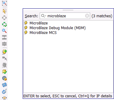
Select the first option (the bare Microblaze) by double-clicking on it. You should see a fancy Microblaze component show up on the block diagarm now.
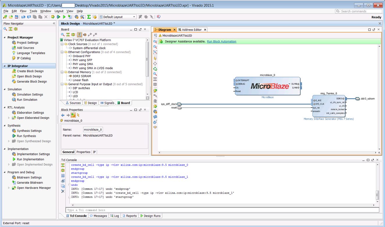
The next step is to configure our processor the way we want it. So click on Run Block Automation at the top of the Block Diagram and set the options as shown in the screenshot below:
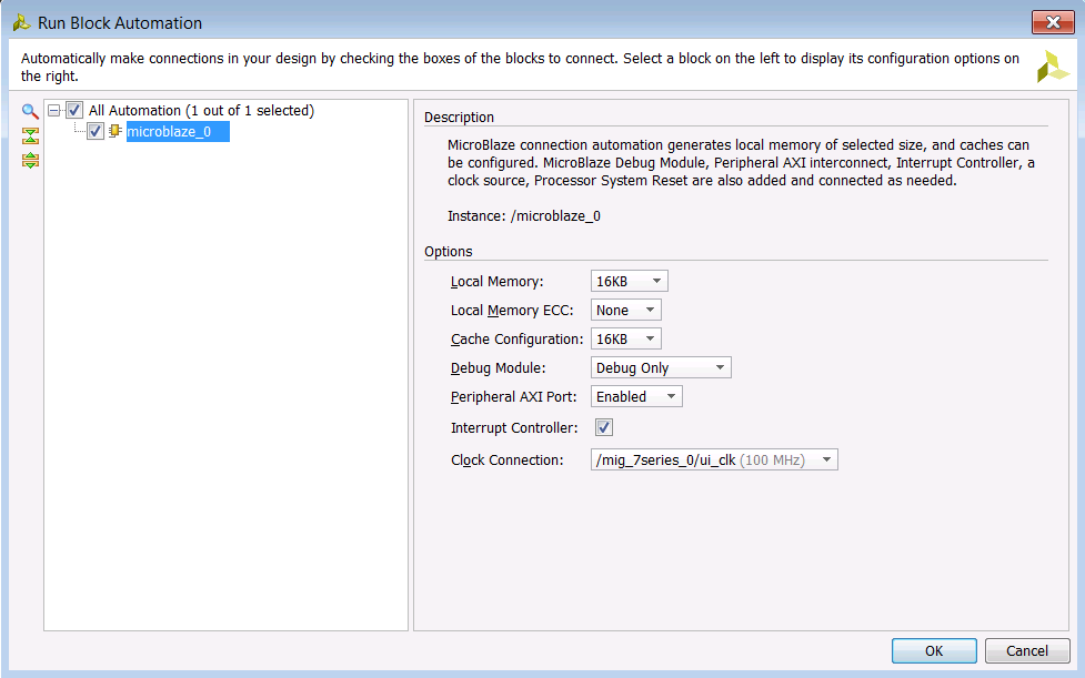
We're upping the Local Memory and Cache to 16 kB (although 8 kB would probably be fine for our application), and we're also going to add an Interrupt Controller so that can detect when we've received a byte over the serial port without having to continuously poll. After selecting these options, click OK and wait for the block automation to complete. You should see a bunch of new components on your block diagram at this point. Specifically, we now have a debug module, a local memory module, an AXI interrupt controller, and an AXI peripheral module.
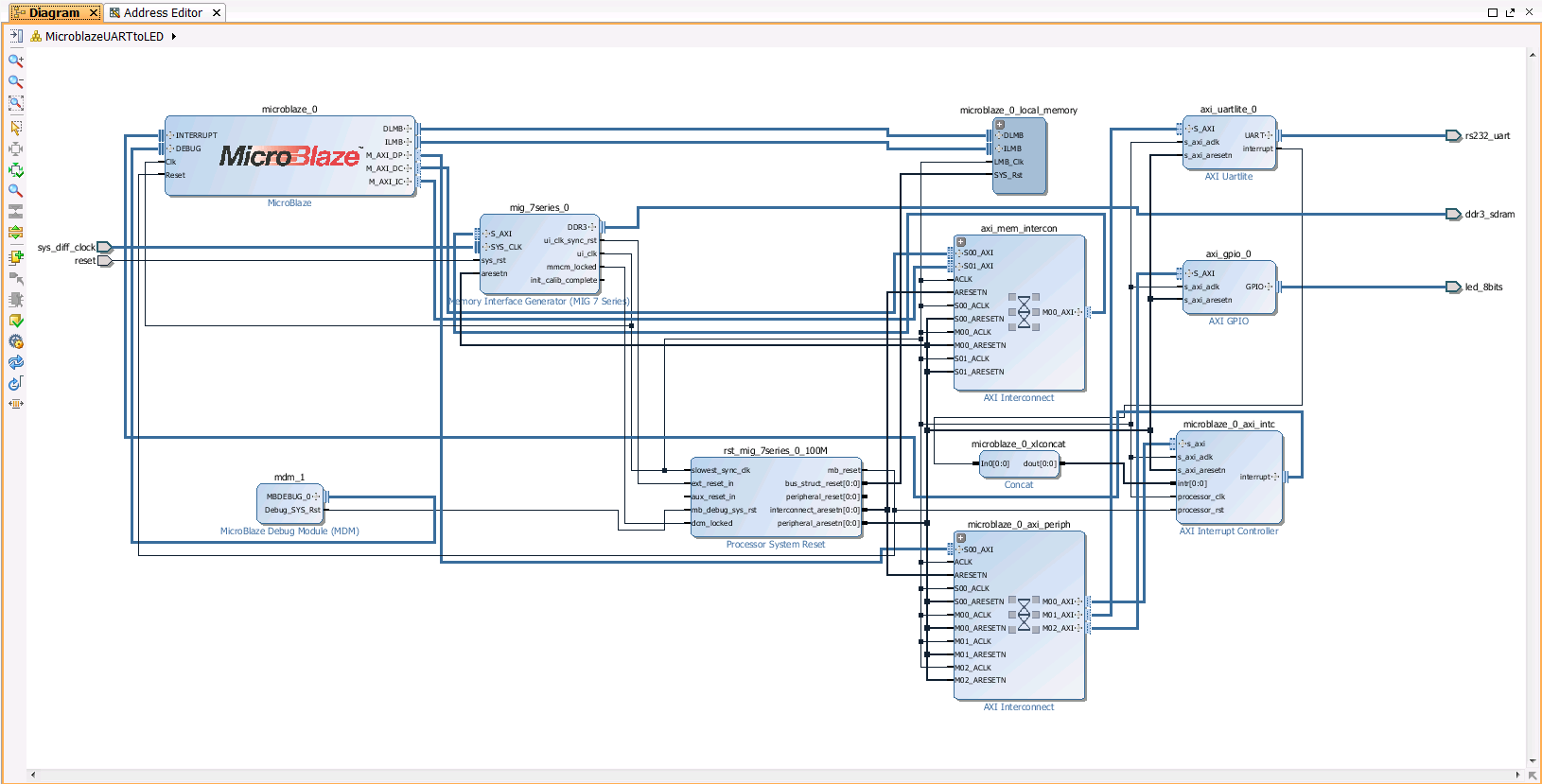
Now we're going to add all the peripherals we want and connect them to our AXI peripheral controller. Go back to the Board tab on the left hand side of the block diagram and find the UART. Drag this onto your block diagram. Then find the LED module under the General Purpose Input or Output heading and drag this onto the block diagram. Notice that after you've done this, a check mark appears next to the modules you've added.
Once you've got the UART and LED components in the block diagram, click on Run Connection Automation and select the checkmark at the top that forces all the boxes to be checked. Click OK to connect everything, and don't worry about the warning about the obsolete connection.
The connection automation isn't smart enough to know that we want the UART to generate interrupts, so we've got to manually make that connection. Highlight the interrupt pin on the UART by clicking on it once. Then right click and select Make Connection. Select the In0 port and click OK. We actually don't really need the concatenation module, but it's a good idea to keep it in case you want to expand on this design later. We can get rid of the second input port by double-clicking on the module and setting the Number of Ports to 1 and clicking OK. Once you do this, you should see the second input port disappear and your block diagram should look like this:
Now that we've got our block design all set up, right click on the diagram and select Validate Design. If you've done everything properly, you should get a message saying that everything is all good.
3.1 Creating an HDL Wrapper
Our design is actually quite useless the way it is now. To make it useful, we need to generate the HDL code that the FPGA understands: the code that will actually create the soft-core processor in the fabric of the chip. To do this, go to the Sources tab on the left hand side and select the Hierarchy sub-tab. Right click on the MicroblazeUARTtoLED icon (the one that looks like a little triangle made of blocks) and select Create HDL Wrapper. You can keep the option to have Vivado manage the wrapper (the default) and press OK.
If everything went according to plan, you should see your block design turn into a little fancy icon with blue and green squares, plus a little circle with a "ve" (for Verilog) next to it. If you expand below, you can see that Vivado has created a lot (and I mean a lot!) of verilog code.
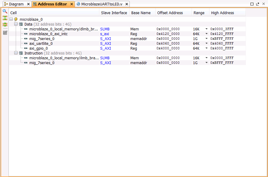
It's worth checking out the Address Editor in the Block Diagram at this point. You can see that Vivado has created a memory map for the GPIO, UART, and interrupt controller, along with the 16 kB of RAM at 0x0000_0000.
The really good news about this project is that Vivado is smart enough to know the layout of the hardware on the VC707 exactly, so we really don't have to do any work specifying the pins for the UART or the GPIOs. If you're working with a different board, you might have to do this.
3.2 Synthesizing, Implementing, and Generating the Bitstream
Now that we've got our HDL wrapper, we can proceed with synthesizing and implementing our design. If you're not familiar with what each of these steps does, it's worth reading up on them (I've got a bit of an explanation in another tutorial). I'll just go through the steps here.
First, click on the Run Synthesis icon under the flow navigator. This should take awhile. I mean, we're building a processor out of a bunch of gates!
Once the synthesis is finished, keep Run Implementation checked and press OK. Again, this will take some time.
After the implementation has been completed, select Generate Bitstream and click OK.
And when we've finally got your bitstream generated, the first step is going to be to program the FPGA with the Microblaze logic we've just created. So click on Open Hardware Manager and then click on Open Target. Follow the prompts in the Open New Hardware Target Wizard to connect to the FPGA if you haven't already set it up.
With the bitstream programmed in the FGPA, now we can export our design to the Xilinx SDK so that the program knows about all the different components we need libraries and source files for. So click on File -> Export -> Export Hardware, and when the window pops up, check the box that says Include Bitstream and then press OK.
Now click on File -> Launch SDK. In the next part of the tutorial, we'll focus on creating an ELF file to run on our freshly created microprocessor!
← Previous ... Next →
Table Of Contents
- Part 1: Getting Started
- Part 2: Creating the Project in Vivado
- Part 3: Creating the Block Diagram
- Part 4: Building the Application in SDK
- Part 5: Running the Application in SDK