7.0 Building the Design
Building our design in Vivado consists of three steps: 1) Elaborating the Design, 2) Synthesizing the Design, and 3) Implementing the Design. We'll go through each step here to get the bitstream we want. I am not going to go into much depth at all because it's way beyond the scope of this tutorial (and because I am not at all sure what is going behind the scenes in Vivado for each of these processes).
7.1 Elaborating the Design
In the Flow Navigator, click on RTL Analysis → Open Elaborated Design . Elaborating the design basically turns your code from raw RTL into a variety of other equivalent visual representations. You can view an RTL Netlist, Schematic, and Graphical Hierarchy. You can also use a "cross-select" feature that will help in debugging and making sure your code represents what you want it to represent.
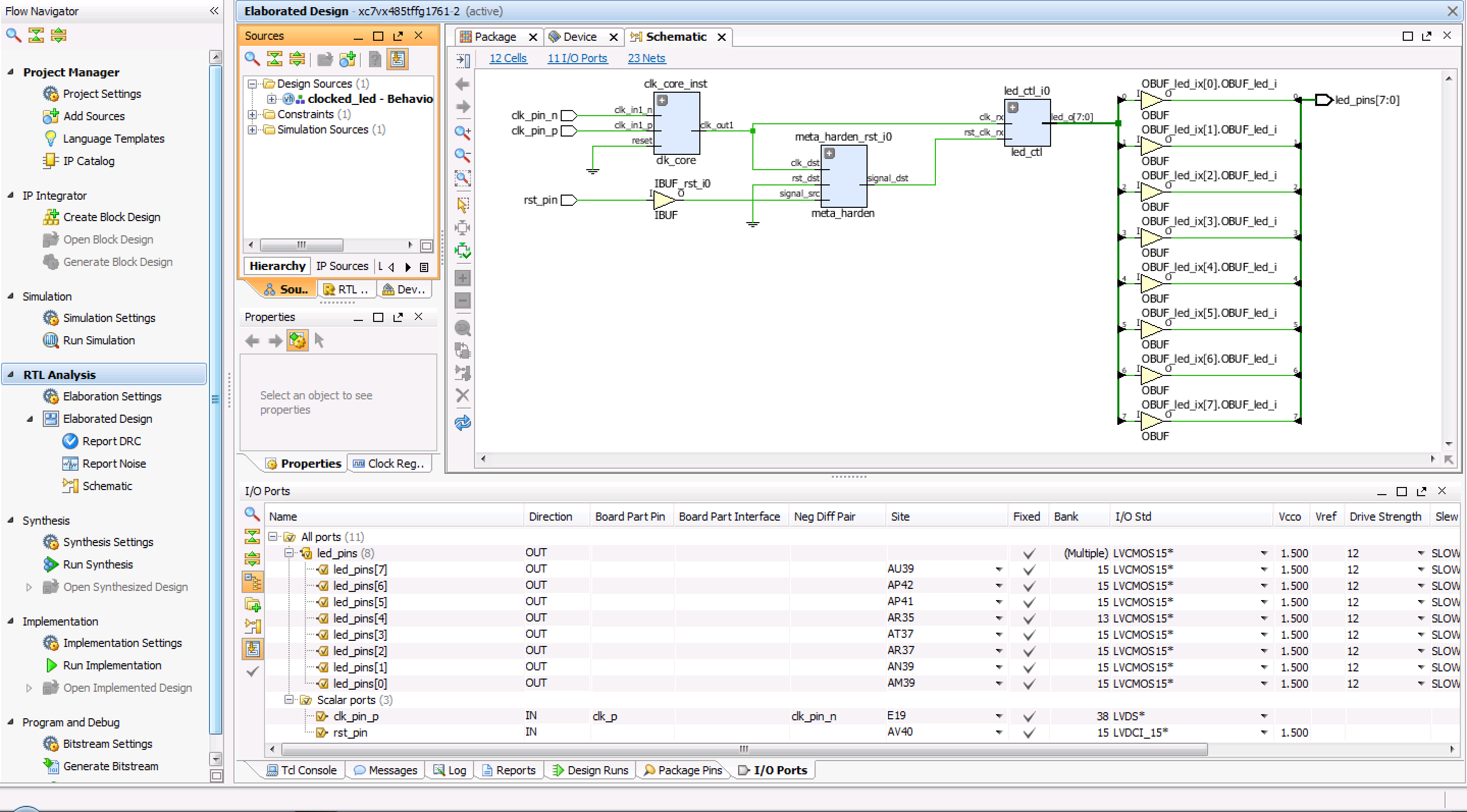
It'll take a bit for the design to be elaborated. Once it's through, you can click on the RTL Analysis → Open Elaborated Design → Schematic to bring up the schematic representation of our design. Also click on the "I/O Ports" tab at the bottom of the Vivado window and you should see something that looks like this:

It's very worthwhile at this point to take a few dozen minutes and explore the elaborated design. Open the Design Hierarchy by selecting Tools → Show Hierarchy to see what Vivado thinks your hierarchy looks like. Look through the Tcl Console tab, look at the Log and the I/O Ports...just get acquainted with where things are located and how Vivado works.
7.2 Synthesizing the Design
The next step is to synthesize the design. Synthesis "is the process of transforming an RTL-specified design into a gate-level representation". So basically this means that it will take your VHDL or Verilog code and a standard cell library (the UNISIM libary and any others you specified in your code) and produce a gate-level netlist as output. The netlist will consist of primitives like Look-Up Tables (LUTs), Flip-Flops, etc.
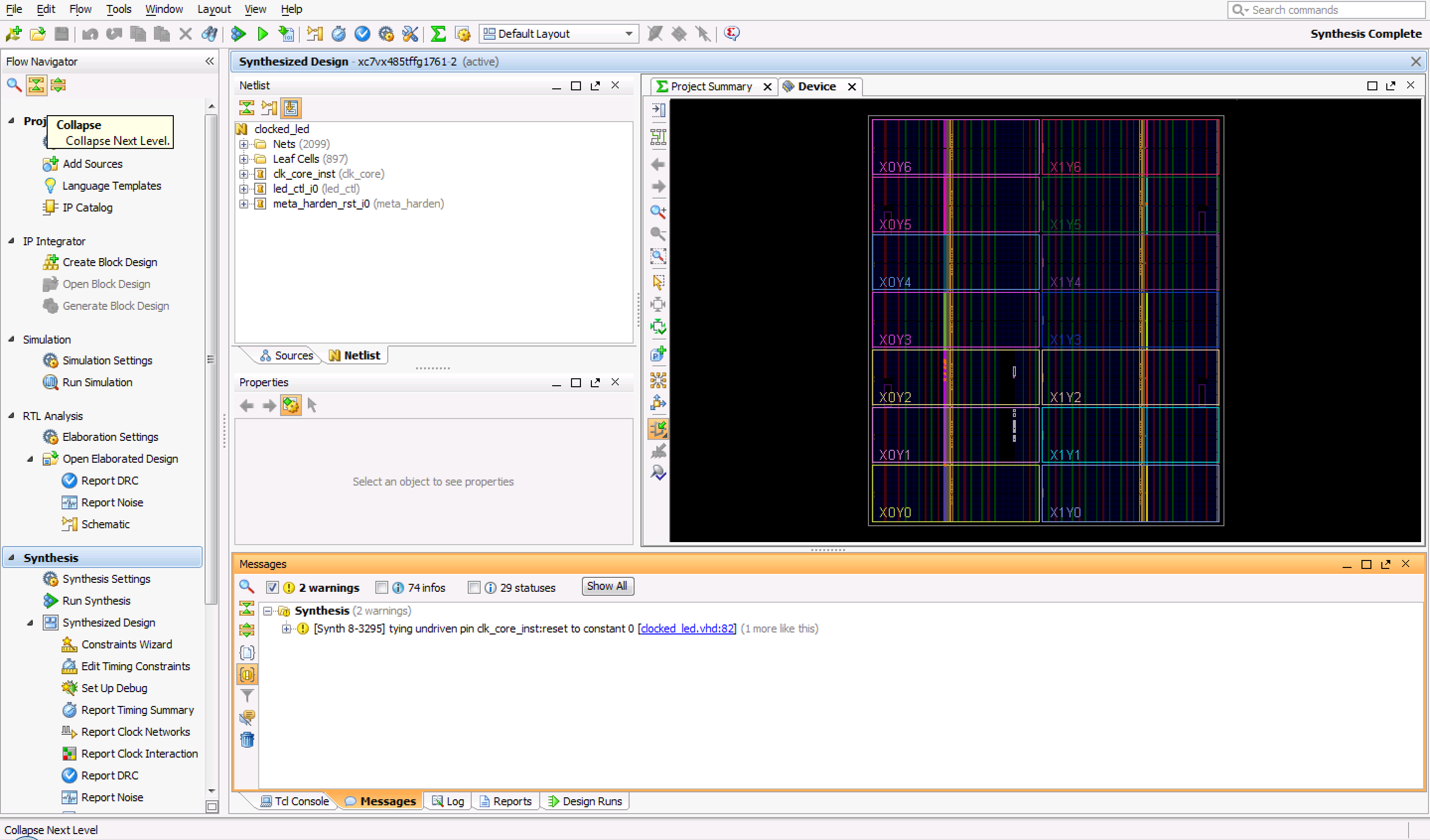
To run the synthesis, just click on Synthesis → Run Synthesis. After it's over, select "Open Synthesized Design" and you'll see the following windows:

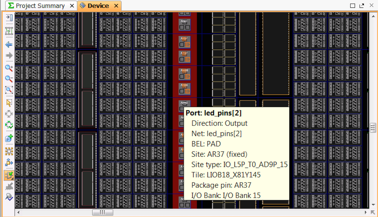
This shows the floorplan of the FPGA and the resources that have been alocated so far. Notice that you don't see much of anything highlighted yet. If you zoom in, you can see that pretty much all that's been laid down are the IO pins you selected in your constraints file and some clock buffers. You can take a closer look by zooming in and panning around in the Device window. If you click on the highlighted resources, you'll get some information just like what's shown in the figure below:

Next you should click on the Project Summary tab and investigate the Utilization. You should see that we're going to be using 1% of the Flip-Flops, 1% of the Look-Up Tables, 2% of the I/Os, 6% of the BUFGs, and 7% of the MMCMs.
7.3 Implementing the Design
The next step is to implement the design. Implementation is basically equivalent to placing and routing. Vivado will use some incredibly fancy and impressive algorithms to place the netlist elements on the FPGA and connect them all together in such a way that all the constraints are met. In my experience, this can be quite a slow process, most likely because " If a route can't be done per the constraints, there follows a rip up, re-map, and re-route phase for that element's path".
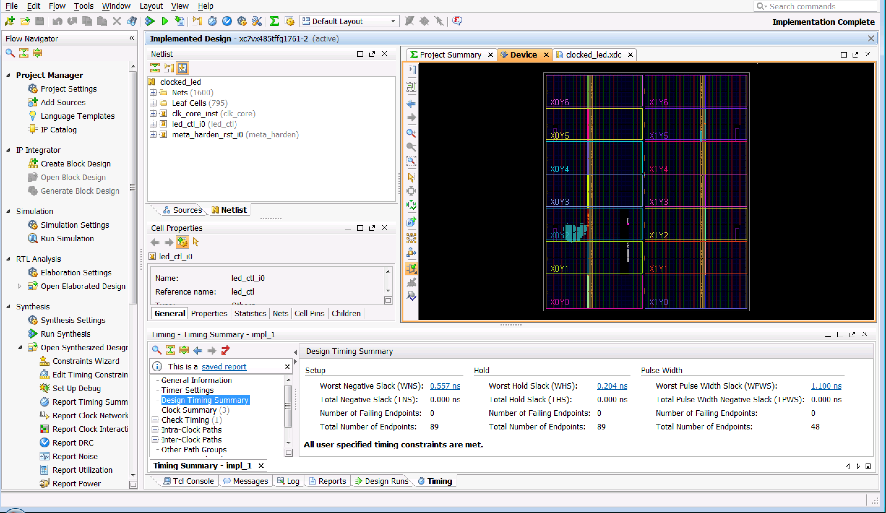
To start the implementation, click on Implementation → Run Implementation. After the implementation has finished, select "Open Implemented Design". You can tell it to close the Synthesized Design since you're not going to be needing it anymore. Notice you've got another FPGA floorplan, but this time there are a whole bunch of resources highlighted. It's beneficial to zoom in and investigate the slices and see what each one does and so forth.

The timing constraints should all be met for the design. However, as I mentioned before, it's useful to see what happens when they aren't. Or maybe I'm just saying that because I spent a while trying to figure it out myself the first time I ran through this exercise :).
To see an easy-to-understand violation of the timing constraints, go down to the bottom of the project window and click on the "Design Runs" tab. Go up to the "synth_1" entry, right click on it, and then selct "Reset Runs". Answer yes when it warns you about also resetting the implementation. You'll also have to click on "close design" at the top when it pops up.
After you've reset everything, set the output frequency of your output clock to 200 MHz by bringing up the clocking wizard again (go to the Sources window, select the IP Sources tab, and double click on "clk_core"). Re-run the implementation and see what happens. You should see that you're got some negative slack and a bunch ugly red text to warn you that you haven't met the timing constraints. Why is this? Hint: you're asking for an awful lot of stuff to be done in between every rising edge of clk_rx. It's not quite as easy as writing software, eh?
When you've had enough of getting errors, set your clock back to 50 MHz and do the implementation again. When it's done, click on "Generate Bitstream". In the next step, we'll download the bitstream to the VC707 with USB-to-JTAG cable and see some LEDs flash.
← Previous ... Next →
Table Of Contents
- Part 1: Getting Started
- Part 2: Creating the Project in Vivado
- Part 3: Taking a Look at the VHDL Source Code
- Part 4: Creating clk_core With the Clocking Wizard
- Part 5: Source Code for the LED Controller
- Part 6: The Constraints File clocked_led.xdc
- Part 7: Elaborating, Synthesizing, and Implementing
- Part 8: Generating and Downloading the Bitstream